We offer Design to Device™ services to deliver our customers’ compound semiconductor photonics requirements.
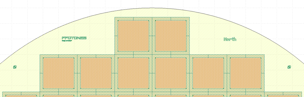
Design
Our in-house design service’s unique selling proposition is in our ability to work closely with our epitaxy partner and fabrication process partners to get designs manufacturing ready.
In our rigorous design process, we run multiple simulation iterations with feedback from epitaxy and fabrication engineers.
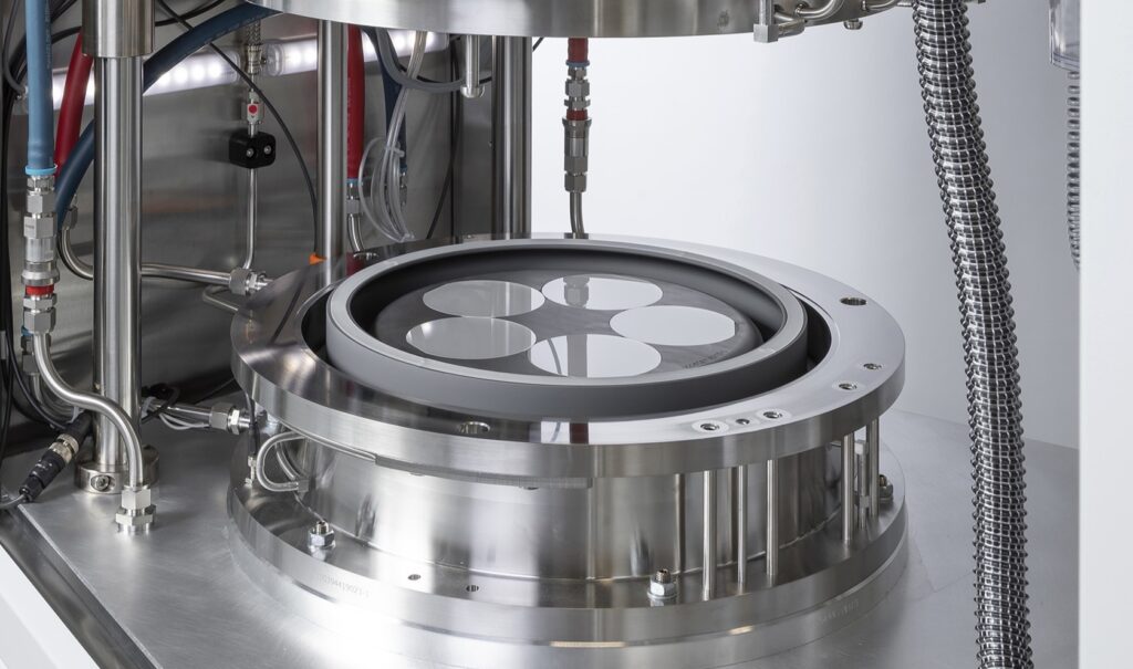
Epitaxy
We work closely with our world class epitaxy partner to grow epi-wafers for our customers. Epitaxial designs are carefully modelled in-house and simulation results used to fine tune epi layer designs according to requirements and hand-in-glove with epitaxy engineers.
Fabrication
We work with local university fabs, leveraging their extensive toolsets and process development experience. Services include full range of photolithography using contact, projection and electron beam tools; PECVD mask deposition; mask and III-V ICP and RIE etch; metal deposition; dicing and others.